Visible to Intel only — GUID: joc1409530785102
Ixiasoft
1.2.2.1.1. Device Selection Section
1.2.2.1.2. Power Rail Data and Configuration Section
1.2.2.1.3. Meeting Target Impedance when Entering 0 A into the PDN Tool
1.2.2.1.4. Dealing with Multiple Shared Power Supply Pin Types
1.2.2.1.5. VRM Data Section
1.2.2.1.6. Rail Group Summary Section
1.2.2.1.7. VRM Impedance Section
1.2.2.1.8. BGA Via Section
1.2.2.1.9. Plane Section
1.2.2.1.10. Spreading Section
1.2.2.1.11. Implementing Split Planes
1.2.2.1.12. FEFFECTIVE Section
1.2.2.1.13. Decoupling Section
1.2.2.1.14. Results Summary Section
1.2.2.1.15. Recommended Flow for Deriving Decoupling for an FPGA System using the System_Decap Tab
Visible to Intel only — GUID: joc1409530785102
Ixiasoft
1.2.3.2. Deriving Decoupling in a Single-Rail Scenario
A power supply connects to only one power rail on the FPGA device in a single-rail scenario. The PDN noise is created by the dynamic current change of the single rail. You determine ZTARGET and FEFFECTIVE based on the parameters related to the selected rail only.
The PDN tool 2.0 provides two ways to derive a decoupling network. You can set up the tool with the information needed and let the tool derive the PDN decoupling for your system. You can also manually enter the information and derive decoupling. To derive the desired capacitor combination:
- Select the device/power rail to work with.
- Select the parameter settings for the PDN components.
- Enter the electric parameters to set ZTARGET and FEFFECTIVE.
You need to have a good estimate of the parameters entered to derive the proper decoupling guidelines (ZTARGET and FEFFECTIVE). Although you need to determine those guidelines based on the worst-case scenario, pessimistic settings result in hard-to-achieve guidelines and over design of your PCB decoupling.
- Derive the PCB decoupling scheme.
You must adjust the number and value of the PCB capacitors in the Decoupling Capacitor (Mid/High Frequency) and Decoupling Capacitor (Bulk) fields to keep the plotted ZEFF below ZTARGET until FEFFECTIVE. You can derive the decoupling for the selected power rail manually. You can also select the Auto Decouple button and let the PDN tool 2.0 automatically determine a decoupling solution. If you are not able to find a capacitor combination that meets your design goal, you can try to change the parameters at 2. For example, you can reduce the BGA via inductance used in the Calculate option by reducing the BGA via length in the BGA_VIA tab and using the low option for plane spreading. These changes reduce parasitic inductance and make it easier to achieve your decoupling goal. To achieve the low spreading setting, you must place the mid to high frequency PCB capacitors close to the FPGA device. You also must minimize the dielectric thickness between the power and ground plane. Refer to Troubleshooting ZEFF if the ZEFF is too high or the number of capacitors for decoupling becomes too high.
If you are not able to meet the ZTARGET requirement with the changes above, the PDN in your design may have reached its physical limitation under the electrical parameters you entered for ZTARGET and FEFFECTIVE. You should re-examine these parameters to check if they are overly pessimistic.
Figure 22. Enlarged Plot of ZEFF This sample impedance plot is for a 1SG280LU_F50 VCC power rail. Assume that the minimum voltage supply is 0.8 V, Idynamic is 50 A, dynamic current change is 30% of Idynamic, and the maximum allowable die noise tolerance is 5% of supply voltage. The VCC rail has 169 power BGA vias. The length of BGA via is assumed to be 20 mil.
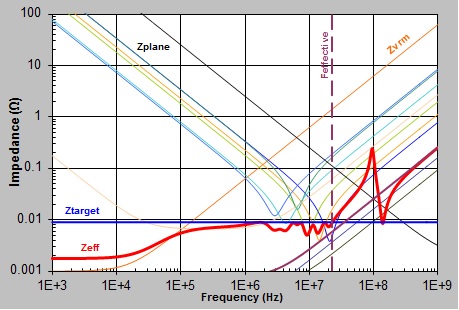
The PDN tool 2.0 calculated that ZTARGET is 0.0027 Ω and FEFFECTIVE is 13.58 MHz. The figure above shows one of the capacitor combinations that you can select to meet the design goal. As shown in the plot, ZEFF remains under ZTARGET up to FEFFECTIVE. There are many combinations, but the ideal solution is to minimize the quantity and the type of capacitors needed to achieve a flat impedance profile below the ZTARGET.
Related Information