1.3.1.9. Viewing the Simulation Results
The simulation testbench prints the results at the transcript or terminal where you execute the simulation script. The following example shows the printout and waveform of the simulation in the ModelSim‐ Intel® FPGA Edition:
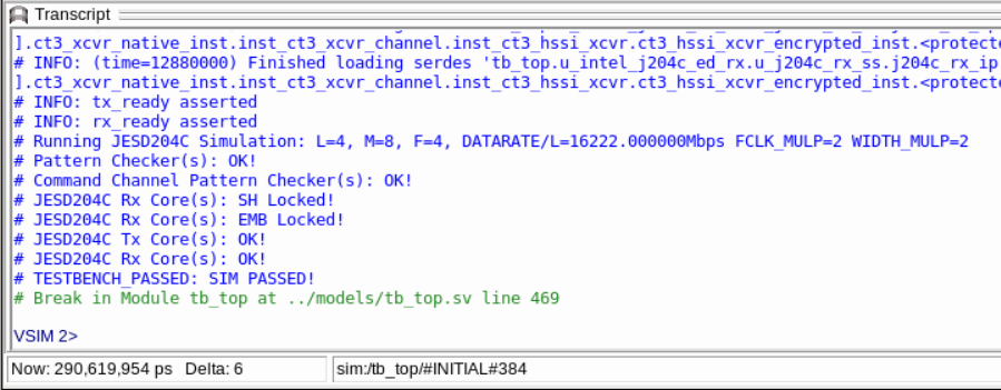
If the simulation passes, the transcript section prints TESTBENCH_PASSED: SIM PASSED! as shown in the following figure.
Figure 11. ModelSim‐ Intel® FPGA Edition Simulation Results Transcript
If the simulation fails, the transcript section prints TESTBENCH_FAILED: SIM FAILED! along with the failure reason.
If you want to view the waveform, the following events occur during link initialization.
- After the /tb_top/ninit_done and global reset are deasserted, the reset sequencer deasserts the resets of the TX and RX transceivers in both Link 0 and Link 1 of the JESD204C Intel® FPGA IPs.
- /tb_top/tx_ready is asserted when the TX transceiver channels of Link 0 and 1 are ready.
- The link reset for TX JESD204C IPs, /tb_top/tx_rst_n, is deasserted when the core IO PLL is locked and intel_jesd204c/tx_pma_ready and intel_jesd204c/tx_ready are asserted.
- When TX channels send data to the RX channels, the RX transceiver channels ready signal, /tb_top/rx_ready, is not asserted. The link reset for the RX JESD204C IPs, /tb_top/rx_rst_n, is asserted.
Figure 12. ModelSim‐ Intel® FPGA Edition Simulation Waveform After Global Reset Deassertion
- When the RX transceiver channels successfully recover the data and clock, /tb_top/rx_ready is asserted.
- The link reset for the RX JESD204C IPs, the /tb_top/rx_rst_n, is deasserted when the core IO PLL is locked and the intel_jesd204c/rx_pma_ready and intel_jesd204c/rx_ready are asserted.
Figure 13. ModelSim‐ Intel® FPGA Edition Simulation Waveform when RX Transceiver Channels are Ready
- The RX transport layer is out of reset when the /tb_top/rx_rst_n is deasserted. The RX transport layer asserts the j204c_rx_avst_ready signal to the JESD204C Intel® FPGA IP.
- The RX JESD204C IPs achieve sync header alignment (j204c_rx_sh_lock is asserted) when 64 consecutive valid sync headers are detected.
- The RX JESD204C IPs achieve extended multiblock alignment (j204c_rx_emb_lock is asserted) when 4 consecutive valid sequences are detected. A valid sequence is defined as correct EoEMB and EoMB values for a full E*32-bit sync transition stream.
- j204c_rx_alldev_lane_align is asserted when both RX JESD204C IPs achieve lane alignment.
- j204c_rx_avst_valid is asserted when the RX transport layer streams user data to the application layer together with the start-of-multiblock (j204c_rx_somb) and start-of-extended-multiblock (j204c_rx_soemb) markers.
- The command channel of the RX JESD204C IP outputs the CRC-12 signal in the sync header stream. No CRC error (j204c_rx_crc_err) is detected. No parity error (j204c_rx_cmd_par_err) is detected at the command channel.
Figure 14. ModelSim‐ Intel® FPGA Edition Simulation Waveform for Successful Link InitializationFigure 15. ModelSim‐ Intel® FPGA Edition Simulation Waveform for No Data Error
- The pattern checker checks the received sample data from the RX transport layer. No error (/tb_top/data_error) is detected.
- The pattern checker checks the received sync header from the RX JESD204C IP. No error (/tb_top/cmd_data_error) is detected.
- No TX and RX link errors or interrupts (/tb_top/tx_link_error and /tb_top/rx_link_error) are being asserted by both TX and RX JESD204C IPs. The testbench asserts the test_passed flag.