Visible to Intel only — GUID: joc1463527329164
Ixiasoft
Intel® Stratix® 10 Devices and Transceiver Channels
PCB Stackup Selection Guideline
Recommendations for High Speed Signal PCB Routing
FPGA Fan-out Region Design
CFP2/CFP4 Connector Board Layout Design Guideline
QSFP+/zSFP/QSFP28 Connector Board Layout Design Guideline
SMA 2.4-mm Layout Design Guideline
Tyco/Amphenol Interlaken Connector Design Guideline
Electrical Specifications
Document Revision History for AN 766: Intel® Stratix® 10 Devices, High Speed Signal Interface Layout Design Guideline
Option 1: Via-In-Pad Topology
Option 2: Dog-bone with GND Cutout at BGA Pad Topology
Option 3: Micro-via Topology
GND Cutout Under BGA Pads in Fan-out Configuration
Comparison of Dog-bone with GND Cutout Under the BGA and Via-in-Pad Configurations
Trace Shape Routing at the BGA Void Area (Tear Drop Configuration)
Visible to Intel only — GUID: joc1463527329164
Ixiasoft
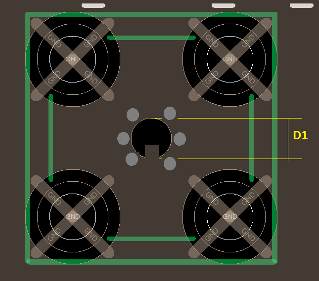
Other 2.4 mm Connectors
Make sure you follow your connector vendor's recommended layout on the PCB at the connector. Intel recommends using a large signal anti-pad on the reference GND plane. Additionally, you should ensure that you have a circle of GND vias and a GND reference diving board.
Figure 94. GND Cutout and Reference Diving BoardFigure shows the first GND layer below the microstrip routing.