6.1.2.1. Simulation Results
This table lists the top-level block contains the input and output ports.
| Ports Name | Ports Type | Descriptions |
|---|---|---|
| clock | Input | System Clock for the encoders, RAM, and decoders. |
| corrupt_dataa_bit0 | Input | Registered active high control signal that 'twist' the zero bit (LSB) of input encoded data at port A before writing into the RAM. 15 |
| address_a data_a wren_a rden_a |
Input | Address input, data input, write enable, and read enable to port A of the RAM. 15 |
| address_b data_b wren_b rden_b |
Input | Address input, data input, write enable, and read enable to port B of the RAM. 15 |
| rdata1 err_corrected1 err_detected1 err_fatal1 |
Output | Output data read from port A of the RAM, and the ECC-status signals reflecting the data read. 16 |
| rdata2 err_corrected2 err_detected2 err_fatal2 |
Output | Output data read from port B of the RAM, and the ECC-status signals reflecting the data read. 16 |
Figure 7. Simulation ResultsThis figure shows the expected simulation waveform results in the ModelSim* - Intel® FPGA Edition software.
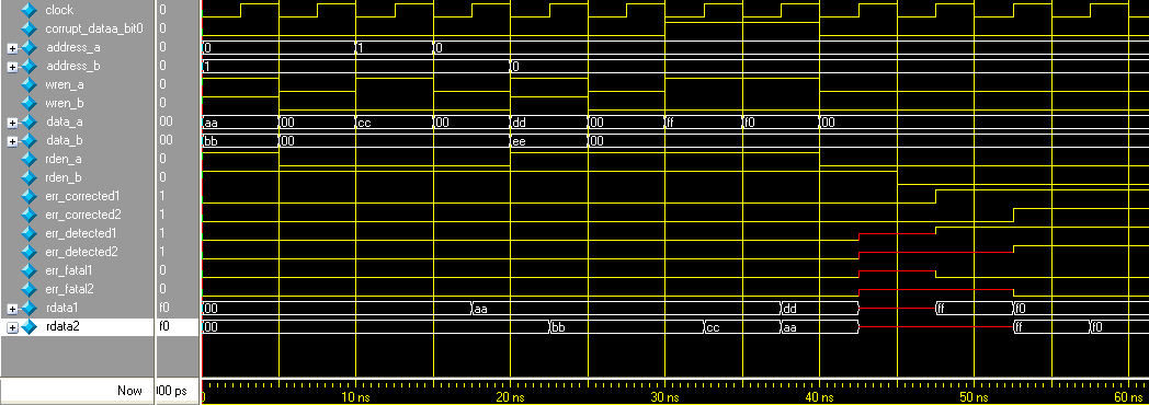
Figure 8. Same-Port Read-During-WriteThis figure shows the timing diagram of when the same-port read-during-write occurs for each port A and port B of the RAM.
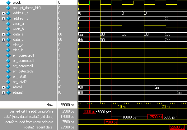
At 2500 ps, same-port read-during-write occurs for each port A and port B. Because the true dual-port RAM configured to port A is reading the new data and port B is reading the old data when the same-port read-during-write occurs, the rdata1 port shows the new data aa and the rdata2 port shows the old data 00 after four clock cycles at 17500 ps. When the data is read again from the same address at the next rising clock edge at 7500 ps, the rdata2 port shows the recent data bb at 22500 ps.
Figure 9. Mixed-Port Read-During-WriteThis figure shows the timing diagram of when the mixed-port read-during-write occurs.
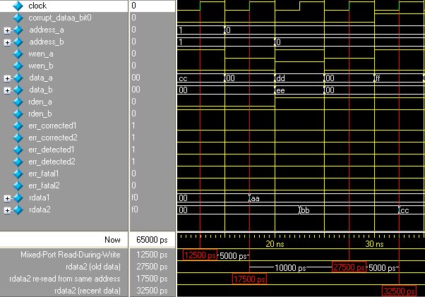
At 12500 ps, mixed-port read-during-write occurs when data cc is both written to port A, and is reading from port B, simultaneously targeting the same address 1. Because the true dual-port RAM that is configured to mixed-port read-during-write is showing the old data, the rdata2 port shows the old data bb after four clock cycles at 27500 ps. When the data is read again from the same address at the next rising clock edge at 17500 ps, the rdata2 port shows the recent data cc at 32500 ps.
Figure 10. Write ContentionThis figure shows the timing diagram of when the write contention occurs.
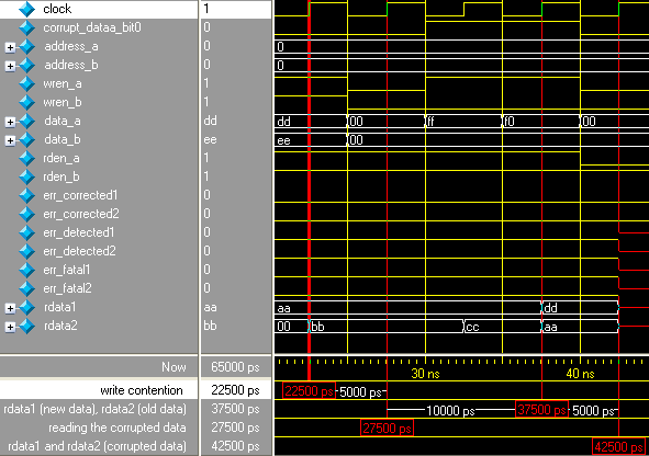
At 22500 ps, the write contention occurs when data dd and ee are written to address 0 simultaneously. Besides that, the same-port read-during-write also occurs for port A and port B. The setting for port A and port B for same-port read-during-write takes effect when the rdata1 port shows the new data dd and the rdata2 port shows the old data aa after four clock cycles at 37500 ps. When the data is read again from the same address at the next rising clock edge at 27500 ps, rdata1 and rdata2 ports show unknown values at 42500 ps. Apart from that, the unknown data input to the decoder also results in an unknown ECC status.
Figure 11. Error Injection– Asserting corrupt_dataa_bit0 This figure shows the timing diagram of the effect when an error is injected to twist the LSB of the encoded data at port A by asserting corrupt_dataa_bit0.
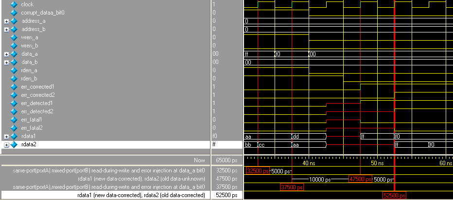
At 32500 ps, same-port read-during-write occurs at port A while mixed-port read-during-write occurs at port B. The corrupt_dataa_bit0 is also asserted to corrupt the LSB of encoded data at port A; therefore, the storing data has the LSB corrupted, in which the intended data ff is corrupted, becomes fe, and stored at address 0. After four clock cycles at 47500 ps, the rdata1 port shows the new data ff that has been corrected by the decoder, and the ECC status signals, err_corrected1 and err_detected1, are asserted. For rdata2 port, old data (which is unknown) is shown and the ECC-status signal remains unknown.
Note: The decoders correct the single-bit error of the data shown at rdata1 and rdata2 ports only. The actual data stored at address 0 in the RAM remains corrupted, until new data is written.
At 37500 ps, the same condition happens to port A and port B. The difference is port B reads the corrupted old data fe from address 0. After four clock cycles at 52500 ps, the rdata2 port shows the old data ff that has been corrected by the decoder and the ECC status signals, err_corrected2 and err_detected2, are asserted to show the data has been corrected.
15 For input ports, only data signal goes through the encoder; others bypass the encoder and go directly to the RAM block. Because the encoder uses one pipeline, signals that bypass the encoder require additional pipelines before going to the RAM. This has been implemented in the top level.
16 The encoder and decoder each use one pipeline while the RAM uses two pipelines, making the total pipeline equal to four. Therefore, read data is only shown at output ports four clock cycles after the read enable is initiated.