2.3.2.4. PCB Via Design
PCB via structures are usually capacitive (fringe coupling from via pads/drill to surrounding reference planes). PCB vias also have via stubs (after back/top drilling to the through-hole vias), which can lower the via impedance even further.
Tuning the via anti-pad size to bring the via impedance to the required impedance tolerance range is essential in via optimization.
However, sometimes there are limitations to increasing the anti-pad size. Due to the ground reference needed for breakout traces, a small anti-pad can make the via impedance go very low.
Here are the techniques that you can take advantage of to control/optimize the PCB via impedance:
- A smaller PCB via anti-pad size results in a lower impedance.
- A longer PCB via stub also results in a lower impedance.
- Smaller PCB via drill sizes result in a higher impedance.
- Smaller PCB via top, bottom, and functional pads result in a higher impedance.
- Thin dielectric layers, i.e. denser planes, result in a lower impedance.
- A higher dielectric constant (Dk) results in a lower impedance.
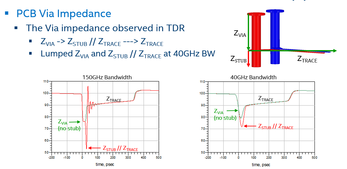
The figure below shows the impedance of PCB vias as measured by TDR. The higher the TDR bandwidth, the more details of the impedance change will be observed. The TDR plot in this figure is from the top via pad to the inner layer trace. The via stub has capacitive characteristics and it reduces the path impedance.
Figure 8. PCB Via Impedance Observation by TDR
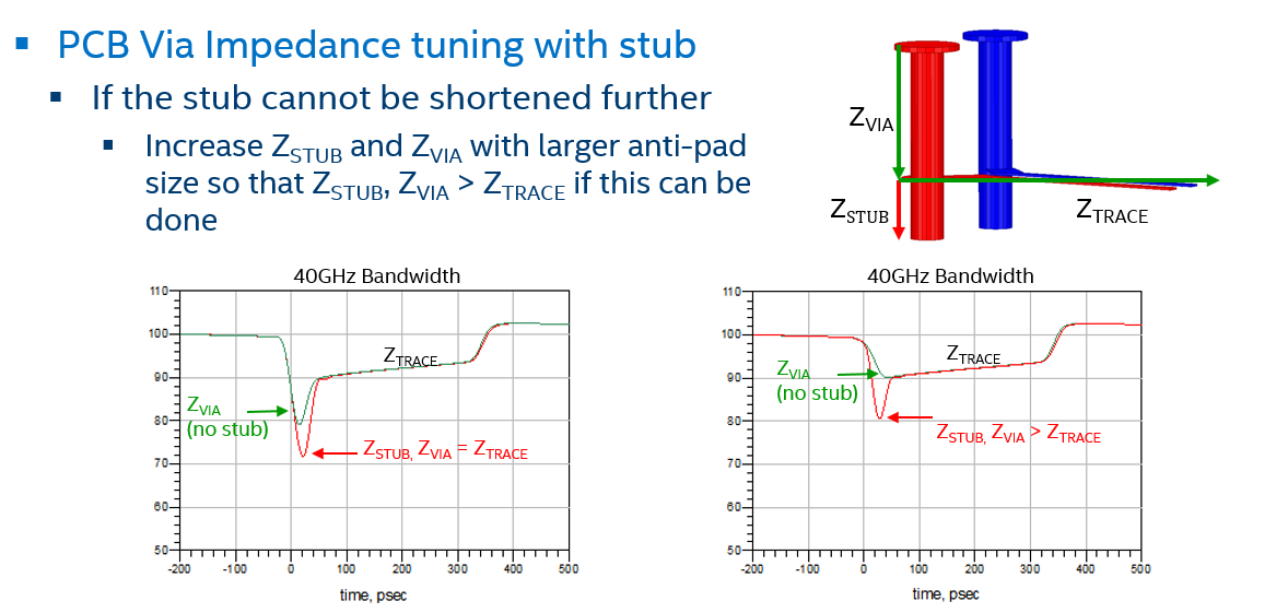
The following figure shows the techniques used for PCB via impedance optimization/tuning. Top/back drilling is essential in high speed data links. However, it may not be possible to shorten the via stub further due to fabrication house limitations. Therefore, achieving a larger anti-pad area would help tune the via impedance to reach a trace impedance with less reflection.
Figure 9. PCB Via Impedance Tuning with Stub
To further tune the PCB via impedance, you must follow the recommendations below:
- Use the smallest via drill/pad allowed in manufacturing to reduce the capacitive coupling that dominates the via impedance discontinuity. Reduce the anti-pad size for better breakout trace ground reference.
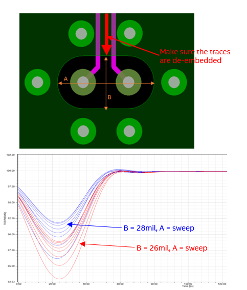
- Sweep the dimensions A and B (refer to the following figure) for the via impedance using any proven commercial 3D E/M tool that works for you.
- The B dimension can impact the breakout trace ground reference, so you should tune A first until you reach the maximum allowable A, then tune B.
Figure 10. PCB Differential Via and TDR Performance with Respect to Various Sweeping Parameters in Via Impedance Control
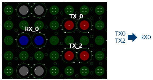
PCB Via Crosstalk
The PCB via pattern follows the package BGA pattern. The via pattern and coupling length directly impact the PCB via coupling . Therefore, it is important to control the via coupling length for different via patterns in order to meet the crosstalk requirements. The 56G PAM4 mode puts a very strict crosstalk limitation (60 dB) on the TX/RX. Referring to the PAM4 usage mode, when channels 2n (n=0, 1, .. 11) run 56G, all other channels are quiet. Therefore, the same channel's TX-to-RX crosstalk, and the next second channel's TX-to-RX crosstalk are among the worst-case crosstalk scenarios in the PCB design. See below worst-case via pattern for TX/RX. For these via transitions, Intel recommends that you control the via coupling length to be smaller than 40 mil.
Figure 11. Worst-Case Via Pattern, 2-TX to 1-RX Crosstalk