1.2. Generating the Design
Figure 3. Procedure
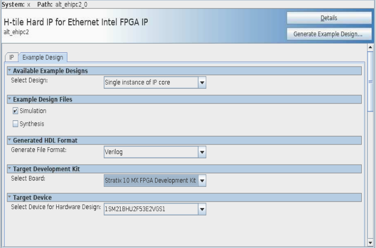
Figure 4. Example Design Tab in the H-Tile Hard IP for Ethernet Intel FPGA IP Parameter Editor
Follow these steps to generate the H-Tile Hard IP for Ethernet Intel FPGA IP hardware design example and testbench:
- If you do not already have an Intel® Quartus® Prime Pro Edition project in which to integrate your H-Tile Hard IP for Ethernet Intel FPGA IP core, you must create one.
- In the Intel® Quartus® Prime Pro Edition, click to create a new Quartus Prime project, or to open an existing Intel® Quartus® Prime project. The wizard prompts you to specify a device.
- Specify the device family Intel Stratix 10 and select a device that meets all of these requirements:
- Transceiver tile is H-tile
- Transceiver speed grade is –1 or –2
- Core speed grade is –1 or –2
- Click Finish.
- In the IP Catalog, locate and select H-tile Hard IP for Ethernet Intel FPGA IP. The New IP Variation window appears.
- Specify a top-level name <your_ip> for your custom IP variation. The parameter editor saves the IP variation settings in a file named <your_ip> .ip.
- Click OK. The parameter editor appears.
- On the IP tab, specify the parameters for your IP core variation.
Important: The design example testbench supports only the default IP parameter settings listed below. Any changes to these settings may cause simulation failure in the testbench.
IP Parameter Settings Default Value Ready latency 0 TX maximum frame size 1518 RX maximum frame size 1518 Enforce maximum frame size Disable Link fault generation option Off Stop TX traffic when link partner send pause No Bytes to remove from RX frames Remove CRC bytes Forward RX pause requests Disable Use source address insertion Disable TX VLAN detection Enable RX VLAN detection Enable PHY Reference Frequency 644.53125 Enable AN/LT Disable Enable Native PHY Debug Master endpoint (NPDME) Disable Enable JTAG to Avalon Master Bridge Disable - On the Example Design tab, under Example Design Files, select the Simulation option to generate the testbench and the compilation-only project. Select the Synthesis option to generate the hardware design example.
Note: You must select at least one of the Simulation and Synthesis options to generate the design example.Note: You must select the Simulation option to generate the testbench.
- On the Example Design tab, under Generated HDL Format, select Verilog HDL or VHDL
Note: If you select VHDL, you must simulate the testbench with a mixed-language simulator. The device under test in the ex_100G directory is a VHDL model, but the main testbench file is a System Verilog file.
- Under Target Development Kit select the Stratix 10 MX FPGA Development Kit to generate the hardware design example. Selecting None generates only the simulation and compilation-only design examples.
Note: The compilation-only and hardware design examples target your project device. For correct hardware design functionality out of the box, you must ensure your project device is the device on your development kit.
- Under Target Device select 1SM21BHU2F53E1VG or 1SM21BHU2F53E2VGS1.
- Click the Generate Example Design button. The Select Example Design Directory window appears.
- If you want to modify the design example directory path or name from the defaults displayed (alt_ehipc2_0_example_design), browse to the new path and type the new design example directory name (<design_example_dir>).