Visible to Intel only — GUID: gvz1618926059132
Ixiasoft
1. About the Video and Vision Processing Suite
2. Getting Started with the Video and Vision Processing IPs
3. Video and Vision Processing IPs Functional Description
4. Video and Vision Processing IP Interfaces
5. Video and Vision Processing IP Registers
6. Video and Vision Processing IPs Software Programming Model
7. Protocol Converter Intel® FPGA IP
8. 1D LUT Intel® FPGA IP
9. 3D LUT Intel® FPGA IP
10. AXI-Stream Broadcaster Intel® FPGA IP
11. Bits per Color Sample Adapter Intel FPGA IP
12. Black Level Correction Intel® FPGA IP
13. Black Level Statistics Intel® FPGA IP
14. Chroma Key Intel® FPGA IP
15. Chroma Resampler Intel® FPGA IP
16. Clipper Intel® FPGA IP
17. Clocked Video Input Intel® FPGA IP
18. Clocked Video to Full-Raster Converter Intel® FPGA IP
19. Clocked Video Output Intel® FPGA IP
20. Color Plane Manager Intel® FPGA IP
21. Color Space Converter Intel® FPGA IP
22. Defective Pixel Correction Intel® FPGA IP
23. Deinterlacer Intel® FPGA IP
24. Demosaic Intel® FPGA IP
25. FIR Filter Intel® FPGA IP
26. Frame Cleaner Intel® FPGA IP
27. Full-Raster to Clocked Video Converter Intel® FPGA IP
28. Full-Raster to Streaming Converter Intel® FPGA IP
29. Genlock Controller Intel® FPGA IP
30. Generic Crosspoint Intel® FPGA IP
31. Genlock Signal Router Intel® FPGA IP
32. Guard Bands Intel® FPGA IP
33. Histogram Statistics Intel® FPGA IP
34. Interlacer Intel® FPGA IP
35. Mixer Intel® FPGA IP
36. Pixels in Parallel Converter Intel® FPGA IP
37. Scaler Intel® FPGA IP
38. Stream Cleaner Intel® FPGA IP
39. Switch Intel® FPGA IP
40. Tone Mapping Operator Intel® FPGA IP
41. Test Pattern Generator Intel® FPGA IP
42. Unsharp Mask Intel® FPGA IP
43. Video and Vision Monitor Intel FPGA IP
44. Video Frame Buffer Intel® FPGA IP
45. Video Frame Reader Intel FPGA IP
46. Video Frame Writer Intel FPGA IP
47. Video Streaming FIFO Intel® FPGA IP
48. Video Timing Generator Intel® FPGA IP
49. Vignette Correction Intel® FPGA IP
50. Warp Intel® FPGA IP
51. White Balance Correction Intel® FPGA IP
52. White Balance Statistics Intel® FPGA IP
53. Design Security
54. Document Revision History for Video and Vision Processing Suite User Guide
29.4.1. Achieving Genlock Controller Free Running (for Initialization or from Lock to Reference Clock N)
29.4.2. Locking to Reference Clock N (from Genlock Controller IP free running)
29.4.3. Setting the VCXO hold over
29.4.4. Restarting the Genlock Controller IP
29.4.5. Locking to Reference Clock N New (from Locking to Reference Clock N Old)
29.4.6. Changing to Reference Clock or VCXO Base Frequencies (switch between p50 and p59.94 video formats and vice-versa)
29.4.7. Disturbing a Reference Clock (a cable pull)
Visible to Intel only — GUID: gvz1618926059132
Ixiasoft
40.3. TMO IP Block Description
The IP accepts RGB-format video input as an Intel FPGA video streaming interface, statistically analyses image content (locally and globally), and dynamically enhances the luma range to improve overall image contrast. This IP enhances input video frame imagery into a well-lit and detailed image.
Figure 103. TMO IP High-level block diagram.
The TMO IP consists of several blocks for video processing, memory, and control. The video datapath includes a luma extractor, image statistics calculator, a soft-processor-based mapping LUT generator, CPU register interface, a contrast enhancement engine, and an image enhancer.
The luma extractor takes an RGB input frame, analyzes it, and extracts luminance. The image statistics calculator takes luma information contained in a video frame and provides a set of global and local statistic parameters regarding the contrast information on the input video frame.
The IP collects local information about the input images in different regions on a video frame, providing the necessary granularity to properly enhance contrast in areas within the video frame that need to be adjusted.
The soft-processor-based mapping LUT generator takes the data gathered from the image statistics calculator block and generates a set of mapping transfer functions. The IP temporarily stores the mapping transfer functions in LUTs to reduce resource utilization footprint.
The contrast enhancement engine applies different amounts of mapping transfer functions in different regions of a video frame, providing the necessary granularity to properly enhance contrast in areas within the frame that you need to adjust. The TMO IP does not use external video frame buffers. Consequently, the contrast enhancement process that the IP applies to the current frame uses statistical information it collects from the previous video frame.
The image enhancer takes the image statics information gathered from the input video frame and with the generated mapping transfer function, it enhances the luma range. The image enhancer calculates a set of weights that it applies to the input RGB data to generate contrast enhanced RGB output video streams.
The embedded Nios® V/g processor used as a mapping LUT generator, is packaged as part of the TMO IP, and customers do not have direct access to it. An external Avalon memory-mapped processor control interface allows you to interact and configure TMO IP, giving them access to the control registers. Because of a higher level of abstraction, a set of software APIs allow you to easily configure and interact with the IP.
You need to get the free license for the Nios V processor to compile the design in Intel Quartus Prime software.
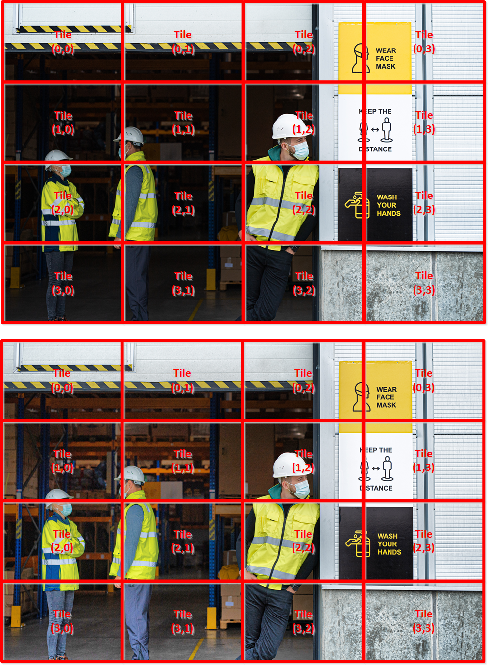
Figure 104. Graphical description of a tile-based histogram generationThe figure shows a graphical description of the tile-based approach, explicitly showing tiles boundaries. Tile boundaries are not visible when you operate the TMO IP. The figure shows them only to demonstrate the IP operation.