Visible to Intel only — GUID: mwh1410471086403
Ixiasoft
1. Simultaneous Switching Noise (SSN) Analysis and Optimizations
2. Signal Integrity Analysis with Third-Party Tools
3. Mentor Graphics* PCB Design Tools Support
4. Cadence PCB Design Tools Support
5. Reviewing Printed Circuit Board Schematics with the Intel® Quartus® Prime Software
A. Intel® Quartus® Prime Standard Edition User Guides
1.1. Simultaneous Switching Noise (SSN) Analysis and Optimizations
1.2. Definitions
1.3. Understanding SSN
1.4. SSN Estimation Tools
1.5. SSN Analysis Overview
1.6. Design Factors Affecting SSN Results
1.7. Optimizing Your Design for SSN Analysis
1.8. Performing SSN Analysis and Viewing Results
1.9. Decreasing Processing Time for SSN Analysis
1.10. Scripting Support
1.112.63.64.75.6. Document Revision History1.112.63.64.75.6. Document Revision History1.112.63.64.75.6. Document Revision History1.112.63.64.75.6. Document Revision History1.112.63.64.75.6. Document Revision History
1.7.1. Optimizing Pin Placements for Signal Integrity
1.7.2. Specifying Board Trace Model Settings
1.7.3. Defining PCB Layers and PCB Layer Thickness
Tcl Commands for Specifying PCB Layer Assignments
1.7.4. Specifying Signal Breakout Layers
1.7.5. Creating I/O Assignments
1.7.6. Decreasing Pessimism in SSN Analysis
1.7.7. Excluding Pins as Aggressor Signals
2.1. Signal Integrity Analysis with Third-Party Tools
2.2. I/O Model Selection: IBIS or HSPICE
2.3. FPGA to Board Signal Integrity Analysis Flow
2.4. Simulation with IBIS Models
2.5. Simulation with HSPICE Models
1.112.63.64.75.6. Document Revision History1.112.63.64.75.6. Document Revision History1.112.63.64.75.6. Document Revision History1.112.63.64.75.6. Document Revision History1.112.63.64.75.6. Document Revision History
2.4.1. Elements of an IBIS Model
2.4.2. Creating Accurate IBIS Models
2.4.3. Design Simulation Using the Mentor Graphics* HyperLynx* Software
2.4.4. Configuring LineSim to Use Intel IBIS Models
2.4.5. Integrating Intel IBIS Models into LineSim Simulations
2.4.6. Running and Interpreting LineSim Simulations
2.5.1. Supported Devices and Signaling
2.5.2. Accessing HSPICE Simulation Kits
2.5.3. The Double Counting Problem in HSPICE Simulations
2.5.4. HSPICE Writer Tool Flow
2.5.5. Running an HSPICE Simulation
2.5.6. Interpreting the Results of an Output Simulation
2.5.7. Interpreting the Results of an Input Simulation
2.5.8. Viewing and Interpreting Tabular Simulation Results
2.5.9. Viewing Graphical Simulation Results
2.5.10. Making Design Adjustments Based on HSPICE Simulations
2.5.11. Sample Input for I/O HSPICE Simulation Deck
2.5.12. Sample Output for I/O HSPICE Simulation Deck
2.5.13. Advanced Topics
2.5.4.1. Applying I/O Assignments
2.5.4.2. Enabling HSPICE Writer
2.5.4.3. Enabling HSPICE Writer Using Assignments
2.5.4.4. Naming Conventions for HSPICE Files
2.5.4.5. Invoking HSPICE Writer
2.5.4.6. Invoking HSPICE Writer from the Command Line
2.5.4.7. Customizing Automatically Generated HSPICE Decks
2.5.12.1. Header Comment
2.5.12.2. Simulation Conditions
2.5.12.3. Simulation Options
2.5.12.4. Constant Definition
2.5.12.5. I/O Buffer Netlist
2.5.12.6. Drive Strength
2.5.12.7. Slew Rate and Delay Chain
2.5.12.8. I/O Buffer Instantiation
2.5.12.9. Board and Trace Termination
2.5.12.10. Double-Counting Compensation Circuitry
2.5.12.11. Simulation Analysis
3.1. FPGA-to-PCB Design Flow
3.2. Integrating with I/O Designer
3.3. Integrating with DxDesigner
3.4. Analyzing FPGA Simultaneous Switching Noise (SSN)
3.5. Scripting API
1.112.63.64.75.6. Document Revision History1.112.63.64.75.6. Document Revision History1.112.63.64.75.6. Document Revision History1.112.63.64.75.6. Document Revision History1.112.63.64.75.6. Document Revision History
3.2.1. Generating Pin Assignment Files
3.2.2. I/O Designer Settings
3.2.3. Transferring I/O Assignments
3.2.4. Updating I/O Designer with Intel® Quartus® Prime Pin Assignments
3.2.5. Updating Intel® Quartus® Prime with I/O Designer Pin Assignments
3.2.6. Generating Schematic Symbols in I/O Designer
3.2.7. Exporting Schematic Symbols to DxDesigner
4.1. Cadence PCB Design Tools Support
4.2. Product Comparison
4.3. FPGA-to-PCB Design Flow
4.4. Setting Up the Intel® Quartus® Prime Software
4.5. FPGA-to-Board Integration with the Cadence Allegro Design Entry HDL Software
4.6. FPGA-to-Board Integration with Cadence Allegro Design Entry CIS Software
1.112.63.64.75.6. Document Revision History1.112.63.64.75.6. Document Revision History1.112.63.64.75.6. Document Revision History1.112.63.64.75.6. Document Revision History1.112.63.64.75.6. Document Revision History
5.1. Reviewing Intel® Quartus® Prime Software Settings
5.2. Reviewing Device Pin-Out Information in the Fitter Report
5.3. Reviewing Compilation Error and Warning Messages
5.4. Using Additional Intel® Quartus® Prime Software Features
5.5. Using Additional Intel® Quartus® Prime Software Tools
1.112.63.64.75.6. Document Revision History1.112.63.64.75.6. Document Revision History1.112.63.64.75.6. Document Revision History1.112.63.64.75.6. Document Revision History1.112.63.64.75.6. Document Revision History
Visible to Intel only — GUID: mwh1410471086403
Ixiasoft
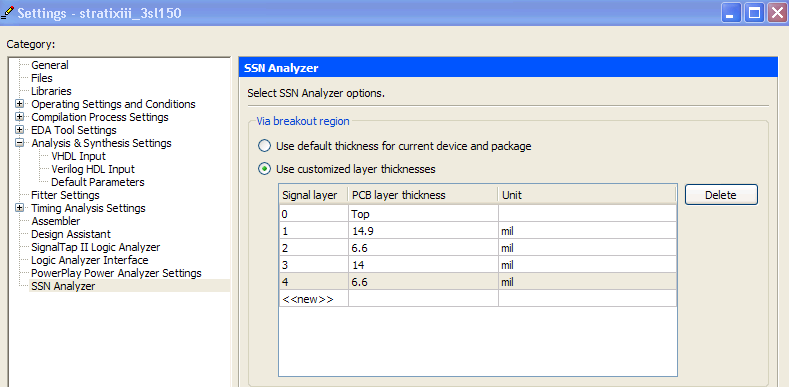
1.7.3. Defining PCB Layers and PCB Layer Thickness
Every PCB is fabricated using a number of layers. To remove some of the pessimism from your SSN results, Altera recommends that you create assignments describing your PCB layers in the Intel® Quartus® Prime software.
You can specify the number of layers on you PCB, and their thickness. The PCB layer information is used only during SSN analysis and is not used in other processes run by the Intel® Quartus® Prime software. If a custom PCB breakout region is not described you can select the default thickness, which directs the SSN Analyzer to use a single-layer PCB breakout region during SSN analysis.
All the assignments you create for the PCB layers are saved to the .qsf. You can also use Tcl commands to create PCB layer assignments. You can create any number of PCB layers, however, the layers must be consecutive.
Tcl Commands for Specifying PCB Layer Assignments
set_global_assignment -name PCB_LAYER_THICKNESS 0.00099822M -section_id 1 set_global_assignment -name PCB_LAYER_THICKNESS 0.00034036M -section_id 2 set_global_assignment -name PCB_LAYER_THICKNESS 0.00034036M -section_id 3
The cross-section shows the stackup information of a PCB, which tells you the number of layers used in your PCB. The PCB shown in this example consists of various signal and circuit layers on which FPGA pins are routed, as well as the power and ground layers.
Figure 9. Snapshot of Stackup of a PCB Shown in the Allegro Board Design Environment
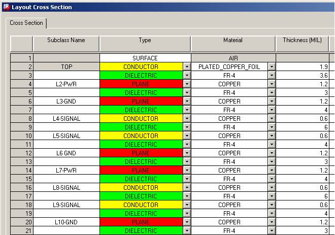
In this example, each of the four signal layers are a different thickness, with the depths shown in the Thickness (MIL) column. The layer thickness for each signal layer is computed as follows:
- Signal Layer 1 is the L4-SIGNAL, at thickness (1.9+3.6+1.2+3+1.2+4=) 14.9 mils
- Signal Layer 2 is the L5-SIGNAL, at thickness (0.6+6=) 6.6 mils
- Signal Layer 3 is the L8-SIGNAL, at thickness (0.6+4+1.2+3+1.2+4=) 14 mils
- Signal Layer 4 is the L9-SIGNAL, at thickness (0.6+6=) 6.6 mils
Figure 10. PCB Layers and Thickness Assignments Specified in the Intel® Quartus® Prime Software