Visible to Intel only — GUID: iga1436549134685
Ixiasoft
3.2. Default Switch and Jumper Settings
This topic shows you how to restore the default factory settings and explains their functions.
CAUTION:
Do not install or remove jumpers (shunts) while the development board is powered on.
Figure 4. Default Switch and Jumper Settings
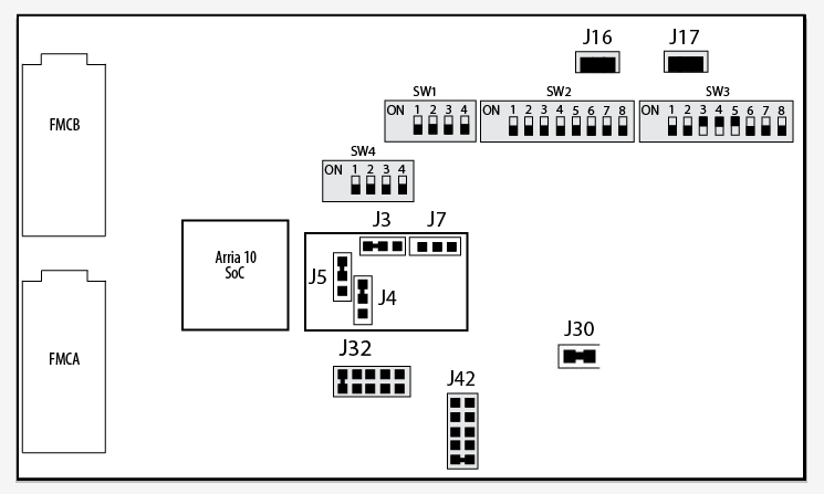
Note: The Switch position is represented by the black box.
To restore the switches to their factory default settings, perform these steps:
- Set the DIP switch bank (SW1) to match the SW1 DIP Switch Settings table and the Default Switch and Jumper Settings figure.
Note: In the following table, ON indicates the switch is to the upper position according to the board orientation as shown in the Default Switch and Jumper Settings figure.
Table 4. SW1 Factory Default Settings Switch Bit Name Bit Function Default Position 1 I2C flag Switch 1.1 has the following options: - ON (0) = System MAX V is the I2C master
- OFF (1) = HPS is the I2C master
OFF 2 DC_POWER_CTRL Switch 1.2 has the following options: - ON (0) = Power off PCIe* slot when it is present
- OFF (1) = Power up PCIe* directly
OFF 3 factory_load Switch 1.3 has the following options: - ON (0) = Load user design from flash at power up
- OFF (1) = Load factory design from flash at power up
OFF 4 security_mode Reserved OFF Table 5. SW4 Switch Settings Switch Bit Name Bit Function Default Position 1 Reserved Reserved OFF 2 MSEL0 Switch 4.2 has the following options: - ON (Up) = MSEL0 is 1
- OFF (Down) = MSEL0 is 0
OFF 3 MSEL1 Switch 4.3 has the following options: - ON (Up) = MSEL1 is 1
- OFF (Down) = MSEL1 is 0
OFF 4 MSEL2 Switch 4.4 has the following options: - ON (Up) = MSEL2 is 1
- OFF (Down) = MSEL2 is 0
OFF Table 6. MSEL Settings for each Configuration Scheme of Intel® Arria® 10 SoC Devices Configuration Vccpgm (V) Power-On Reset (POR delay) Valid MSEL [2:0] JTAG-based configuration - - Use any valid MSEL pin settings below AS-Active Serial (x1 and x4) 1.8 Fast 010 Standard 011 PS-Passive Serial 1.2/1.5/1.8 Fast 000 Standard 001 - Set the DIP switch bank (SW3) to match the following tables:
Table 7. SW3 Factory Default Settings Switch Board Label Function Default Position 1 Intel® Arria® 10 ON- Intel® Arria® 10 JTAG Bypass
OFF- Intel® Arria® 10 JTAG Enable
OFF 2 IO MAX® V ON- MAX V JTAG Bypass
OFF- MAX V JTAG EnableOFF 3 FMCA ON- FMCA JTAG Bypass
OFF- FMCA JTAG Enable
ON 4 FMCB ON- FMCB JTAG Bypass
OFF- FMCB JTAG Enable
ON 5 PCIe* ON- PCIe* JTAG Bypass
OFF- PCIe* JTAG Enable
ON 6 MSTR0 On-Board Intel® FPGA Download Cable II JTAG Master OFF 7 MSTR1 On-Board Intel® FPGA Download Cable II JTAG Master OFF 8 MSTR2 On-Board Intel® FPGA Download Cable II JTAG Master OFF - Set the following jumper blocks to match the table below:
Table 8. Default Jumper Settings Board Reference Board Label Description Default Position J16, J17 OSC2_CLK_SEL - 00 (SHORT, SHORT): Selects the on-board 25MHz clock
- 01 (SHORT, OPEN): Selects SMA clock which connected to J15
- 10 (OPEN, SHORT): Selects the on-board 33MHz clock
- 11 (OPEN, OPEN): none
SHORT, SHORT J30 HPS Core Voltage - SHORT: HPS core 0.95 V
- OPEN: HPS core 0.9 V
SHORT J32 Voltage of FMCBVADJ - No SHORT: 1.1 V
- SHORT 1 and 2: 1.2 V
- SHORT 3 and 4: 1.25 V
- SHORT 5 and 6: 1.35 V
- SHORT 7 and 8: 1.5 V
- SHORT 9 and 10: 1.8 V
SHORT 9 and 10 J42 Voltage of FMCAVADJ - No SHORT: 1.1 V
- SHORT 1 and 2: 1.1 V
- SHORT 3 and 4: 1.2 V
- SHORT 5 and 6: 1.35 V
- SHORT 7 and 8: 1.5 V
- SHORT 9 and 10: 1.8 V
SHORT 9 and 10
Related Information
1 The directions of these pins are in reference to the board arrangement as in the Default Switch and Jumper Settings figure.