Test Results
The following table contains the possible results and their definition.
| Result | Definition |
|---|---|
| PASS | The Device Under Test (DUT) was observed to exhibit conformant behavior. |
| PASS with comments | The DUT was observed to exhibit conformant behavior. However, an additional explanation of the situation is included, such as due to time limitations only a portion of the testing was performed. |
| FAIL | The DUT was observed to exhibit non-conformant behavior. |
| Warning | The DUT was observed to exhibit behavior that is not recommended. |
| Refer to comments | From the observations, a valid pass or fail could not be determined. An additional explanation of the situation is included. |
The following table shows the results for test cases CGS.1, CGS.2, ILA.1, ILA.2, ILA.3, TL.1, and SCR.1 with different values of L, M, F, K, subclass, data rate, sampling clock, link clock, and SYSREF frequencies.
| Test | L | M | F | SCR | K | Lane rate (Gbps) | DAC IQ rate (MSPS) | Link Clock (MHz) | Result |
|---|---|---|---|---|---|---|---|---|---|
| 1 | 1 | 2 | 4 | 0 | 32 | 6.144 | 153.6 | 153.6 | PASS with comments |
| 2 | 1 | 2 | 4 | 1 | 32 | 6.144 | 153.6 | 153.6 | PASS with comments |
| 3 | 2 | 2 | 2 | 0 | 32 | 6.144 | 307.2 | 153.6 | PASS with comments |
| 4 | 2 | 2 | 2 | 1 | 32 | 6.144 | 307.2 | 153.6 | PASS with comments |
| 5 | 4 | 2 | 1 | 0 | 32 | 3.072 | 307.2 | 76.8 | PASS with comments |
| 6 | 4 | 2 | 1 | 1 | 32 | 3.072 | 307.2 | 76.8 | PASS with comments |
| 7 | 1 | 4 | 8 | 0 | 32 | 6.144 | 76.8 | 153.6 | PASS with comments |
| 8 | 1 | 4 | 8 | 1 | 32 | 6.144 | 76.8 | 153.6 | PASS with comments |
| 9 | 2 | 4 | 4 | 0 | 32 | 6.144 | 153.6 | 153.6 | PASS with comments |
| 10 | 2 | 4 | 4 | 1 | 32 | 6.144 | 153.6 | 153.6 | PASS with comments |
| 11 | 4 | 4 | 2 | 0 | 32 | 6.144 | 307.2 | 153.6 | PASS with comments |
| 12 | 4 | 4 | 2 | 1 | 32 | 6.144 | 307.2 | 153.6 | PASS with comments |
| Test | L | M | F | SCR | K | Lane rate (Gbps) | ADC IQ rate (MSPS) | Link Clock (MHz) | Result |
|---|---|---|---|---|---|---|---|---|---|
| 1 | 1 | 2 | 4 | 0 | 32 | 6.144 | 153.6 | 153.6 | Pass |
| 2 | 1 | 2 | 4 | 1 | 32 | 6.144 | 153.6 | 153.6 | Pass |
| 3 | 2 | 2 | 2 | 0 | 32 | 3.072 | 153.6 | 76.8 | Pass |
| 4 | 2 | 2 | 2 | 1 | 32 | 3.072 | 153.6 | 76.8 | Pass |
| 5 | 1 | 4 | 8 | 0 | 32 | 6.144 | 76.8 | 153.6 | Pass |
| 6 | 1 | 4 | 8 | 1 | 32 | 6.144 | 76.8 | 153.6 | Pass |
| 7 | 2 | 4 | 4 | 0 | 32 | 6.144 | 153.6 | 153.6 | Pass |
| 8 | 2 | 4 | 4 | 1 | 32 | 6.144 | 153.6 | 153.6 | Pass |
| 9 | 4 | 4 | 2 | 0 | 32 | 3.072 | 153.6 | 7.68 | Pass |
| 10 | 4 | 4 | 2 | 1 | 32 | 3.072 | 153.6 | 7.68 | Pass |
The following table shows the results for test cases DL.1 and DL.2 with different values of L, M, F, K, subclass, data rate, sampling clock, link clock and SYSREF frequencies
| Test | L | M | F | Sub- class | SCR | K | Transmitter Lane rate (Gbps) | Receiver Lane rate (Gbps) | SYSREF pulse frequency 15 (MHz) | Total Latency Result |
|---|---|---|---|---|---|---|---|---|---|---|
| 1 | 1 | 2 | 4 | 1 | 1 | 32 | 6.144 | 6.144 | 0.48 | Pass (1.146 us) |
| 2 | 2 | 2 | 2 | 1 | 1 | 32 | 6.144 | 3.072 | 0.48 | Pass (1.328-1.341 us) |
| 3 | 4 | 2 | 1 | 1 | 1 | 32 | 3.072 | -16 | 0.48 | Pass 16 (0.651-0.657 us) |
| 4 | 1 | 4 | 8 | 1 | 1 | 32 | 6.144 | 6.144 | 0.48 | Pass (2.331 us) |
| 5 | 2 | 4 | 4 | 1 | 1 | 32 | 6.144 | 6.144 | 0.48 | Pass (1.133-1.146 us) |
| 6 | 4 | 4 | 2 | 1 | 1 | 32 | 6.144 | 3.072 | 0.48 | Pass (1.328-1.354 us) |
Figure 10. Oscilloscope plot observed at DAC output.The LO frequency is set to 400MHz in AD9371 RF transmitter in this example and a monotone of 7.68MHz is being transmitted from FPGA.
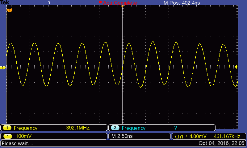
Figure 11. Spectrum Analyzer plot observed at DAC output.The LO frequency is set to 400MHz in AD9371 RF transmitter in this example and a monotone of 7.68MHz is being transmitted from FPGA. The peak is observed at 392.32 MHz (i.e., 400-7.68 MHz).
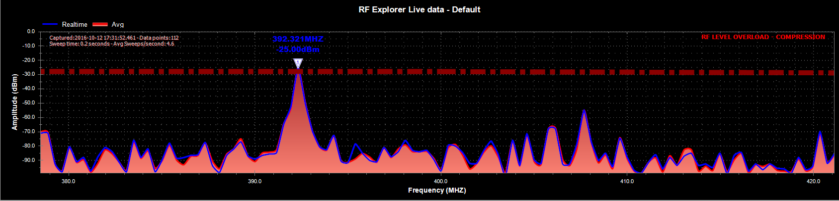
Figure 12. Transmitted sine wave at input of transmitter transport layer and Received sine wave at output of receiver transport layer observed in Signal Tap II Logic Analyzer for mode LMF=148.
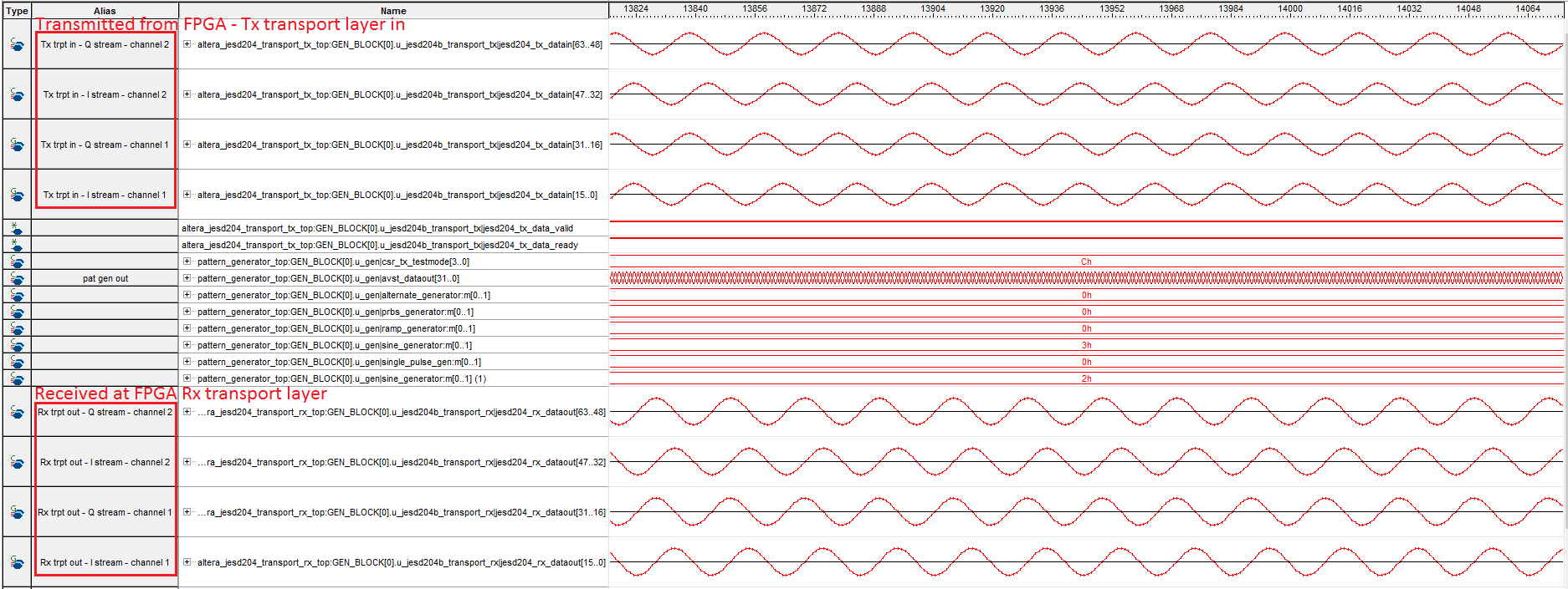
Figure 13. Latency measured between rising edge of transmitted single pulse and rising edge of received single pulse for mode LMF=148. Latency is observed to be 179 rxframe_clk cycles or 2.331 us.
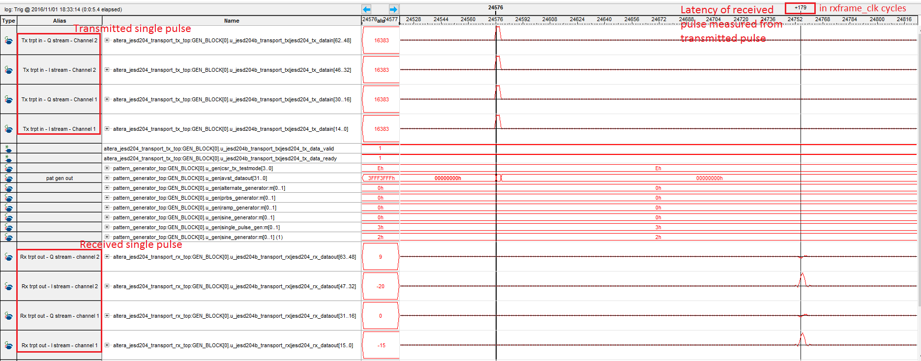
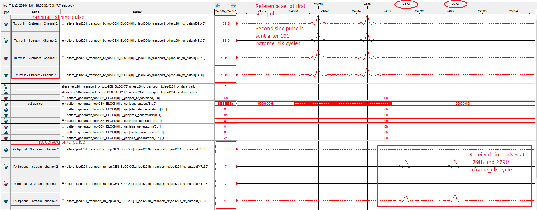
Figure 14. Latency measured between centre of transmitted sinc pattern and centre of received sinc pattern for mode LMF=148.Two pulses are sent with 100 rxframe_clk cycles delay. Same delay of 100 clock cycles is observed in received signal.
15 The sysref frequency is taken as integer multiple of LMFC period. The value of 0.48MHz is derived as a common integer multiple for all JESD204B modes.
16 The link latency is measured as the loopback delay of transmitter and receiver datapaths. For more information on how DL validation is performed on mode with LMF=421, refer to the section on deterministic latency.