Visible to Intel only — GUID: nik1412546929408
Ixiasoft
5.1. Understanding the Design Steps for CvP Initialization Mode
5.2. Understanding the Design Steps for CvP Initialization Mode with the Revision Design Flow
5.3. Understanding the Design Steps for CvP Update Mode
5.4. Bringing Up the Hardware
5.5. CvP Debugging Check List
5.6. Known Issues and Solutions
5.2.1. Downloading and Generating the High Performance Reference Design
5.2.2. Workaround for a Known Issue with Transceiver Reconfiguration Controller IP Core
5.2.3. Creating an Alternate user_led.v File for the Reconfigurable Core Region
5.2.4. Setting up CvP Parameters for CvP Initialization Mode
5.2.5. Creating CvP Revisions of the Core Logic Region Using the CvP Revision Design Flow
5.2.6. Compiling both the Base and cvp_app Revisions in the CvP Revision Design Flow
5.2.7. Splitting the SOF File for the CvP Initialization Mode with the CvP Revision Design Flow
5.3.1. Downloading and Generating the High Performance Reference Design
5.3.2. Workaround for a Known Issue with Transceiver Reconfiguration Controller IP Core
5.3.3. Creating an Alternate user_led.v File for the Reconfigurable Core Region
5.3.4. Setting up CvP Parameters for CvP Update Mode
5.3.5. Creating CvP Revisions of the Core Logic Region Using the CvP Revision Design Flow
5.3.6. Compiling the Design for the CvP Update Mode
5.3.7. Splitting the SOF File for the CvP Update Design Mode
5.3.8. Splitting the SOF File for the CvP Update Mode with the CvP Revision Design Flow
6.3.1. Altera-defined Vendor Specific Capability Header Register
6.3.2. Altera-defined Vendor Specific Header Register
6.3.3. Altera Marker Register
6.3.4. CvP Status Register
6.3.5. CvP Mode Control Register
6.3.6. CvP Data Registers
6.3.7. CvP Programming Control Register
6.3.8. Uncorrectable Internal Error Status Register
6.3.9. Uncorrectable Internal Error Mask Register
6.3.10. Correctable Internal Error Status Register
6.3.11. Correctable Internal Error Mask Register
Visible to Intel only — GUID: nik1412546929408
Ixiasoft
5.4.5. Programming CvP Images and Validating the Link
For CvP initialization mode, you must load the periphery image (top.periph.jic) and then download the core image core image (top.core.rbf) using the PCIe Link. You can use JTAG to load different programming files (i.e. .sof/.jic/periph.pof) into your selected CvP initialization enabled Stratix® V, Cyclone® V , or Arria® V device.
After loading the periphery image via the JTAG port, the link should reach the expected data rate and link width. You can confirm the PCIe link status using the RW Utilities. Then, you can update the core image (top.core.rbf) using the quartus_cvp command over the PCIe link.
For CvP update mode, you first program the FPGA using the .sof or .pof image. After the programming completes the FPGA enters user mode. You can now reconfigure the core image ( .core.rbf), the quartus_cvp command or your own driver.
Follow these steps to program and test the CvP functionality:- Plug in the Stratix V GX FPGA Development Kit to the PCI Express slot of the DUT PC and power it on. Altera recommends that you use the external power supply that the development kit includes.
- On the host PC, open the Quartus Prime Tools menu and select Programmer. The Programmer appears.
Figure 50. Quartus Prime Programmer Settings
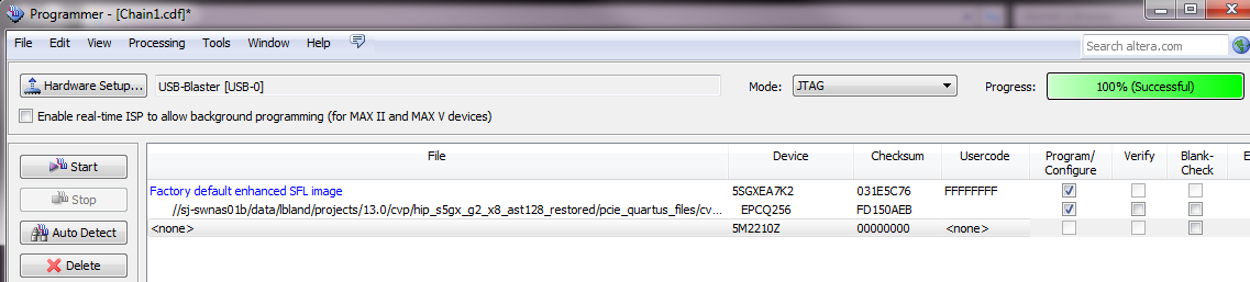
- Click Auto Detect to verify that the USB Blaster recognizes the Stratix V FPGA.
- Follow these steps to program the periphery image:
- Select Stratix V device, then right click None under File column.
- Navigate to pcie_quartus_files/top.periph.jic and click Open.
- Under Program/Configure column, select 5SGXEA7K2 and EPCQ256.
- Click Start to program the periphery image to EPCQ256 flash.
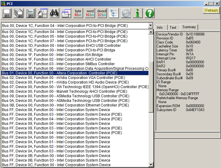
- To force the host PC to re-enumerate the link with the new image, reboot/power cycle the DUT PC.
- You can use RW Utilities or another system software driver to verify the link status. The following figure shows that the RW Utilities enumeration includes an Altera PCIe on Bus 01.
Figure 51. RW Everything Transcript
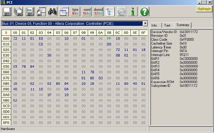
- You can also confirm expected link speed and width. For this Gen1 x1 example design, the following figure shows that both Altera EP Link Capability Register at 0x8C and Link Status register at 0x92 have value 0x11, which confirms the link successfully comes up as Gen1 x1.
Figure 52. Checking Link Status
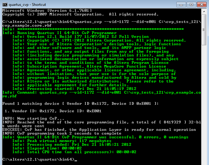
- Follow these steps to program the core image (top.core.rbf) into the FPGA:
- Open a DOS command window.
- Change to appropriate Quartus Prime bin install directory. Both 64-bit and 32-bit bin directories are available. This example uses C:\altera\13.0 \quartus\bin64.
- Type the following command to program the core image. The value of Vendor ID (vid) and Device ID (vid) are in hexadecimal and must match the values you specified on the Device Identification Registers tab of the Stratix V Hard IP for PCI Express IP Core GUI :
quartus_cvp --vid=1172 --did=e001 <path>/top.core.rbf
- The figure below shows the results of successful CvP programming.
Figure 53. Transcript from quartus_cvp Command
If you implement your own software driver to program the core image, refer to the CvP Driver Support section in Chapter 6 of CvP User Guide.If you are using the OpenSource Linux driver, perform the following steps to program the core image:- Copy the .core.rbf file to your working directory.
- Open a console in Linux. Change directory to the same mentioned above where the file is copied.
- Program the core image by typing the following command:
cp *.core.rbf /dev/altera_cvp
You are now ready to run your own tests.
Related Information